NVIDIA Tesla V100 unveiled; 12nm FinFET, 5120 CUDA cores
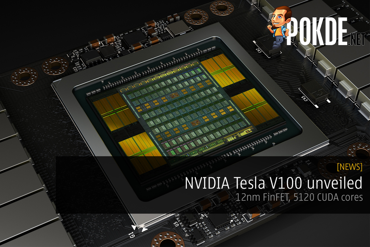
Just when you thought NVIDIA will take a break after launching the GeForce GTX 1080 Ti, a cut-down Titan X with faster clocks, and the Titan Xp, which is a full GP102 with more cores and faster clocks, NVIDIA pulls yet another GPU out of their hat. This time, it’s a whole new architecture, Volta. Say hello to the Tesla V100, the first GPU based on NVIDIA’s latest Volta architecture.
Volta is no longer a new name among hardware enthusiasts, and has already been in NVIDIA’s roadmap for some time. While we have previously assumed Volta will have to stick to 16nm while waiting for TSMC’s 10nm to mature, it seems that NVIDIA has opted for a customized 12nm FinFET manufacturing process at TSMC. Along with this new manufacturing process, the Taiwanese GPU giant packed 21.1 billion transistors on a 815mm2 die for the GV100. By comparison, the Titan Xp just crams 12 billion on 471mm2 of silicon. The GV100 is the largest GPU TSMC can manufacture, and ranks among the largest chips ever manufactured.
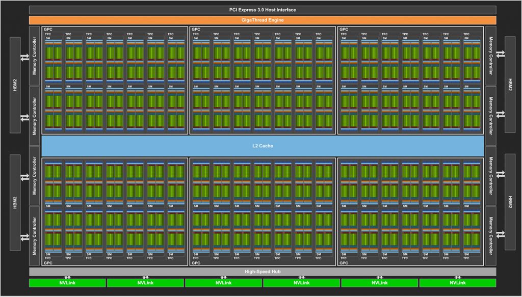
The Tesla V100 will feature 80 SMs, each with 64 CUDA cores, yielding a total of 5120 CUDA cores. For comparison purposes, the Tesla P100 offers 56 SMs with 64 CUDA cores per SM, for a total of 3584 CUDA cores. In addition to these CUDA cores, the Tesla V100 will also feature new tensor cores, a new type of core designed specifically to enhance performance in deep learning operations. Each SM will sport 8 Tensor Cores, which gives you 640 Tensor Cores here. With these new cores, the Tesla V100 is first to the line to break 100 TFLOPS of deep learning performance.
HBM2 memory makes an appearance again, with 16GB of it clocked at 1.75GHz, fed by a 4096-bit bus for a mind-blowing 900GB/s of bandwidth. The Tesla V100 will feature the new NVLink 2 standard, promising 25GB/s bidirectional link bandwidth, up from NVLink’s 20GB/s. There are also 6 NVLink connectors here on the Tesla V100, 2 more than the Tesla P100 has.
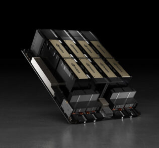
Interested? Eight of these Tesla V100s will be available in the NVIDIA DGX-1V server, for $149 000 (~RM647 850), with a PCIe version later.
Pokdepinion: I wonder how will the Volta consumer GPUs turn out. Will we have yet another massive leap in performance and efficiency, and finally HBM2 in NVIDIA gaming cards?
















Leave a Response