
Cadence and Samsung Foundry have announced an expanded multi-year collaboration focused on advanced semiconductor development for AI infrastructure, high-performance computing (HPC), and physical AI applications. The agreement broadens the availability of memory and interface IP while extending certification of Cadence’s digital design, custom design, 3D-IC, and system design and analysis workflows for Samsung Foundry’s second-generation 2nm process technology.
Cadence Deepens Collaboration With Samsung Foundry
The collaboration builds on work announced in 2025 and expands Cadence’s portfolio of memory and interface IP, including support for NVIDIA NVLink-C2C-enabled interconnects, CUDA-X GPU-accelerated libraries, high-speed SerDes, PCIe, UCIe, and memory interfaces optimized for Samsung’s second-generation 2nm node. The companies stated that the expanded platform is intended to support increasingly complex AI, HPC, and advanced system designs while addressing performance, power efficiency, and development timelines.
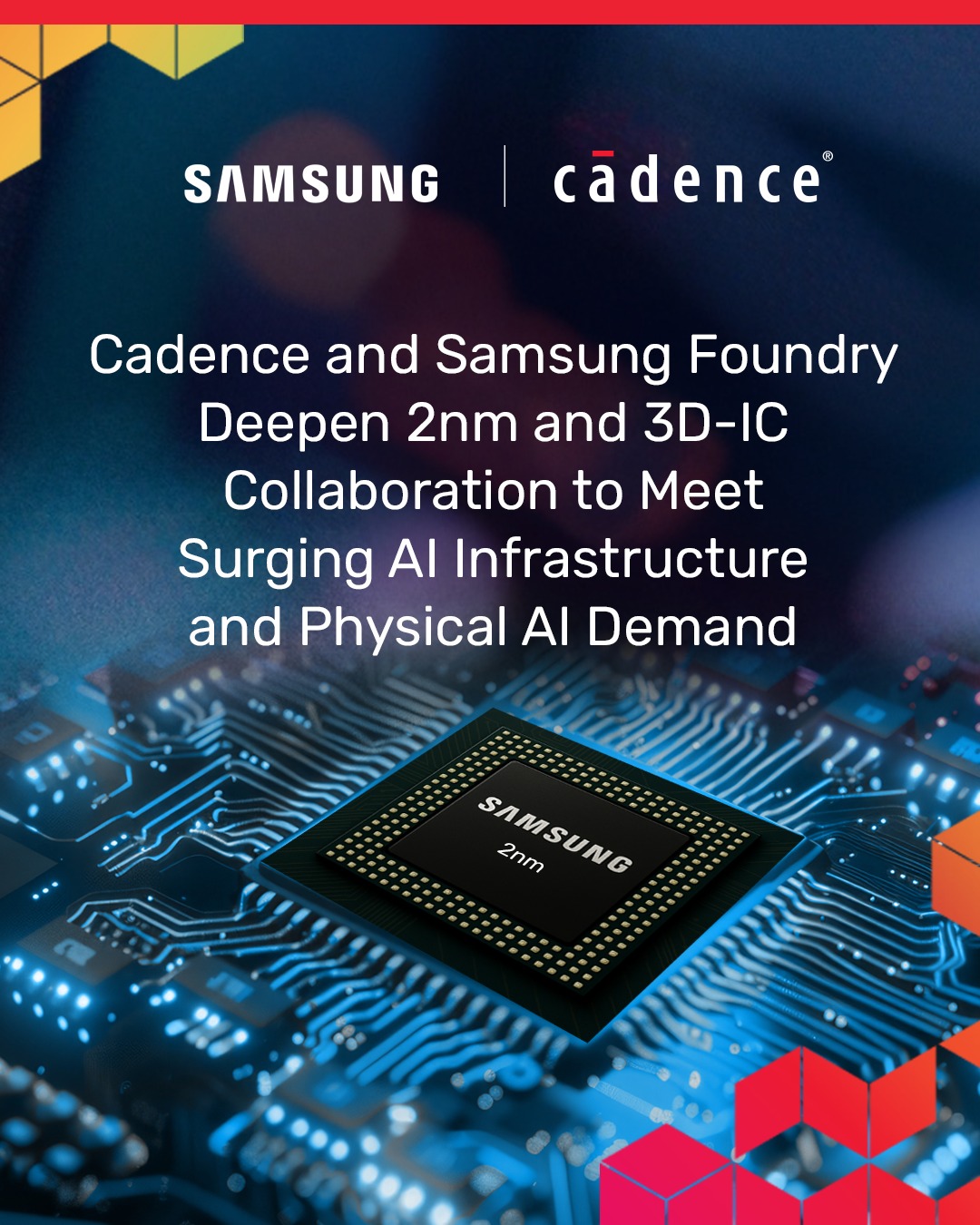
As part of the partnership, Cadence’s certified design environment for Samsung’s 2nm process includes the Innovus Implementation System, Virtuoso Studio, Integrity 3D-IC Platform, Voltus IC Power Integrity Solution, Quantus Extraction Solution, and Tempus Timing Solution. The workflow also incorporates optimization features for power, performance, area, and turnaround time, alongside support for hierarchical design methodologies.
The collaboration further extends to Samsung’s 3D Cube-H packaging technology, enabling a complete planning, implementation, verification, and signoff flow for hybrid copper bonding-based 3D-IC designs. Supported tools include Cerebrus Intelligent Chip Explorer, Integrity 3D-IC, Innovus, Voltus, and Pegasus Verification System, providing capabilities such as silicon interposer auto-routing and design optimization.
NVIDIA is among the companies utilizing the expanded platform to support next-generation AI infrastructure development. The ecosystem integrates NVLink-C2C interconnect technology and CUDA-X GPU-accelerated capabilities to address increasing design complexity associated with advanced-node semiconductor development and high-bandwidth AI computing systems.
Ambarella is also leveraging the collaboration for its next-generation 2nm edge AI platform targeting robotics, drones, autonomous machines, and intelligent sensing applications. The company is utilizing PCIe 5.0 IP and the jointly developed design platform to support the development of low-power AI perception and edge computing processors.
Cadence and Samsung Foundry are expected to showcase the latest developments from the partnership during the Samsung Advanced Foundry Ecosystem (SAFE) 2026 event, where both companies will demonstrate second-generation 2nm and 3D-IC design workflows aimed at GPU-accelerated AI workloads.



Pokdepinion: Race to 2nm is on!
![[COMPUTEX 2026] Acer Presents New Predator & Nitro Gaming Laptops And Gaming Handhelds - 28](https://cdn.pokde.net/wp-content/uploads/2026/06/06231835/acerpredatorcpx26cover.jpg "[COMPUTEX 2026] Acer Presents New Predator & Nitro Gaming Laptops And Gaming Handhelds - 29")
![[COMPUTEX 2026] Synology Showcases AI-Ready Data Management And Protection Solutions - 30](https://cdn.pokde.net/wp-content/uploads/2026/06/06234529/synologycpx26cover.jpg "[COMPUTEX 2026] Synology Showcases AI-Ready Data Management And Protection Solutions - 31")