
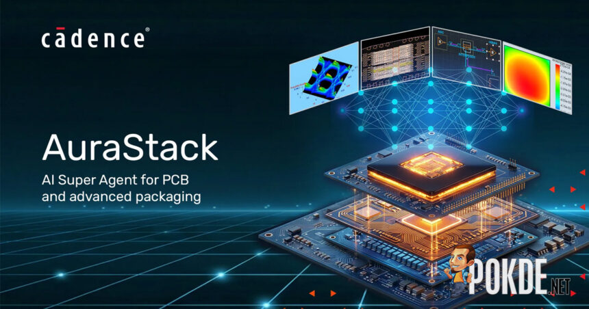
Cadence has introduced the AuraStack AI Super Agent as its latest agentic AI platform designed for printed circuit board (PCB) and advanced packaging design, running on Cadence Allegro AI Studio. The platform is said to cover the design process from system planning through to final product within a single AI-based environment.
Cadence AuraStack AI Super Agent Revealed
The AuraStack AI Super Agent is accelerated by NVIDIA Blackwell and NVIDIA CUDA-X and coordinates AI agents across planning, implementation and multiphysics analysis domains. Cadence stated the platform extends its existing agentic AI offerings, which include the ChipStack, InnoStack and ViraStack AI Super Agents, giving the company agentic AI coverage across digital and analog silicon design, advanced packaging and PCB design.
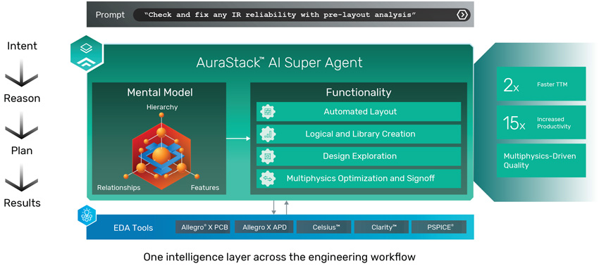
The agent combines agentic AI with simulation and optimization tools across system planning, constraints management, physical structure definition, intellectual property (IP) reuse, place-and-route, design for manufacturability and multiphysics analysis. Cadence said the platform introduces a unified multiphysics foundation that models electrical, thermal and mechanical behavior concurrently, covering areas such as signal and power integrity (SI/PI), thermal performance, mechanical stress, drop, vibration and fatigue analysis.
According to Cadence, the platform is designed to accelerate time-to-market by a factor of two and productivity by a factor of 15, while unifying engineering teams around a shared multiphysics-aware design environment. The platform integrates existing Cadence multiphysics tools, including the Celsius Thermal Solver, Clarity 3D Solver, MSC Nastran and Marc finite element analysis solvers, and the Sigrity X Platform.
Cadence said several companies are working with it to apply AuraStack workflows to packaging and PCB design projects. Tim Costa, vice president and general manager of computational engineering at NVIDIA, said the AuraStack AI Super Agent combined with NVIDIA’s Millennium M2000 Supercomputer delivers multiphysics performance up to 20x faster than previous methods.
Aveek Sarkar, director of the Ecosystem and Alliance Management Division at TSMC, said the companies’ collaboration on substrate auto-routing has increased productivity by a factor of 100 while maintaining quality comparable to manual routing, as part of joint work supporting TSMC’s 3DFabric technologies through the Open Innovation Platform ecosystem.
Pokdepinion: While chip development gets faster, can the raw resources keep up?